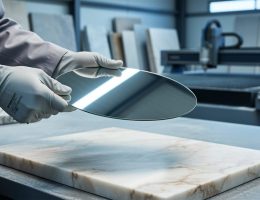
Precision manufacturing transforms raw materials into intricate products through methodical, controlled processes. The semiconductor industry exemplifies this principle at its most extreme: producing microchips requires tolerances measured in nanometers, cleanroom environments thousands of times purer than hospital operating rooms, and multi-billion dollar facilities. Yet the fundamental concepts behind semiconductor fabrication offer surprising relevance for anyone working with precision materials, including natural stone professionals seeking to refine their craft.
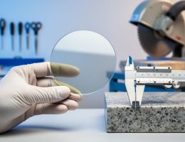
Semiconductor manufacturing begins with ultra-pure silicon wafers …
How Semiconductor Manufacturing Mirrors Stone Fabrication (And What It Teaches Us)
The precision required to manufacture semiconductors rivals the exactness demanded in cutting and finishing premium natural stone. Both industries measure tolerances in microns, depend on contamination-free environments, and transform raw materials into products where a single imperfection can mean total failure.
Silicon wafers progress through hundreds of individual steps across weeks or months, accumulating layers of materials just nanometers thick. Each photolithography cycle, chemical deposition, and etching process must achieve near-perfect accuracy. The parallels to stone fabrication are striking. A granite slab destined for a…
