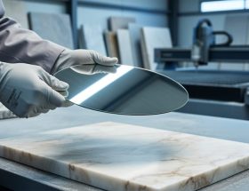
The precision required to manufacture semiconductors rivals the exactness demanded in cutting and finishing premium natural stone. Both industries measure tolerances in microns, depend on contamination-free environments, and transform raw materials into products where a single imperfection can mean total failure.
Silicon wafers progress through hundreds of individual steps across weeks or months, accumulating layers of materials just nanometers thick. Each photolithography cycle, chemical deposition, and etching process must achieve near-perfect accuracy. The parallels to stone fabrication are striking. A granite slab destined for a high-end kitchen undergoes similarly rigorous inspection, where natural variations must be evaluated, cut lines calculated to the millimeter, and surface finishes applied with exacting consistency.
Understanding semiconductor manufacturing offers stone professionals unexpected insights into process control and quality assurance. The cleanroom protocols that prevent microscopic particles from ruining billion-dollar chip production mirror the careful environment management needed when working with light-colored marbles susceptible to staining. The statistical process control methods that semiconductor fabs use to track yield rates can inform how fabricators monitor edge quality, seam alignment, and finish consistency across multiple installations.
This connection between advanced electronics and ancient materials isn’t just academic. Both fields confront the same fundamental challenge: how to reliably produce flawless results from imperfect starting materials. Silicon ingots contain trace impurities that must be controlled. Natural stone arrives with inherent fissures, color variations, and structural irregularities that require expert assessment.
The semiconductor industry’s relentless focus on eliminating defects, standardizing procedures, and measuring every variable provides a framework that stone professionals can adapt. The principles of precision manufacturing transcend specific materials, whether you’re etching transistors onto silicon or shaping limestone for an architectural masterpiece.
The Foundation: What Semiconductor Manufacturing Actually Is
At its core, semiconductor manufacturing transforms pure silicon into the intricate computer chips that power everything from smartphones to industrial control systems. The process shares surprising similarities with precision stone fabrication techniqueswhere raw materials undergo meticulous transformation into functional products through carefully controlled steps.
Semiconductors are materials with electrical conductivity between conductors (like copper) and insulators (like glass). Silicon dominates this field because engineers can precisely control its electrical properties, making it ideal for creating the transistors that form the building blocks of modern electronics. A single microchip can contain billions of these microscopic switches, each smaller than a virus.
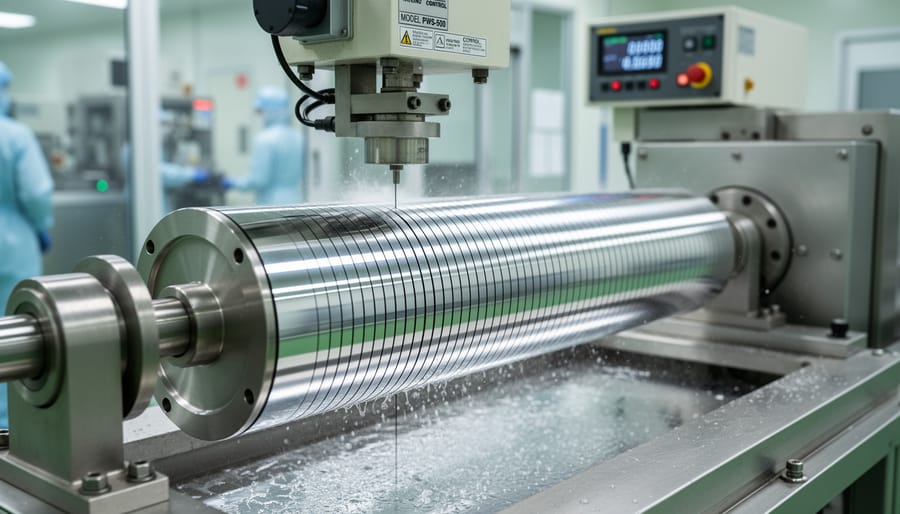
The manufacturing journey begins with ultra-pure silicon extracted from sand, refined to 99.9999999% purity (that’s nine nines). This silicon gets melted and slowly crystallized into cylindrical ingots, which are then sliced into thin circular wafers, typically 300mm in diameter. These wafers serve as the foundation for hundreds of individual chips.
Understanding the fundamental terminology helps demystify this complex process:
- Wafer
- A thin, circular slice of crystalline silicon that serves as the substrate for building integrated circuits. Think of it as the canvas where microscopic electronic components are constructed layer by layer.
- Lithography
- The process of transferring circuit patterns onto the wafer using ultraviolet light, similar to how a photographer develops images. This step defines where components will be placed with nanometer precision.
- Deposition
- Adding thin layers of materials onto the wafer’s surface, building up the chip structure atom by atom or molecule by molecule.
- Etching
- Selectively removing material to create the three-dimensional structures and pathways that form transistors and connections. This subtractive process works in concert with deposition’s additive approach.
- Doping
- Introducing controlled impurities into specific silicon regions to modify their electrical properties, creating the positive and negative zones necessary for transistor function.
These core processes repeat hundreds of times, each cycle adding complexity and functionality. The entire journey from raw wafer to finished chip typically takes two to three months, passing through facilities cleaner than hospital operating rooms.

From Raw Material to Refined Product: The Parallel Journey
Material Selection and Purity Standards
The semiconductor industry transforms ordinary beach sand into silicon crystals that achieve staggering 99.9999999% purity, nine nines. That’s comparable to finding a single grain of impurity in an Olympic swimming pool. Silicon must be purified to semiconductor grade through multiple chemical processes before it’s suitable for chip production, because even microscopic contamination ruins electrical properties.
Stone fabricators recognize this obsession with material purity. When sourcing marble or granite blocks, professionals examine crystal structure, veining patterns, and mineral composition with similar scrutiny. A premium Carrara marble block undergoes rigorous grading based on color consistency, fracture patterns, and the absence of iron deposits that could oxidize. While stone doesn’t require nine-nines purity, top-tier architectural projects demand blocks free from hairline fissures, color variations, or structural weaknesses that compromise longevity.
Both industries employ sophisticated detection methods. Semiconductor manufacturers use spectroscopy and electron microscopes to identify atomic-level defects. Stone professionals rely on ultrasonic testing, visual inspection under controlled lighting, and water absorption tests to reveal hidden flaws. The parallel is striking: whether growing a silicon ingot or selecting a travertine slab, the material’s initial quality determines every subsequent fabrication step. Defects identified early save time and money. Those missed become expensive failures during final production.
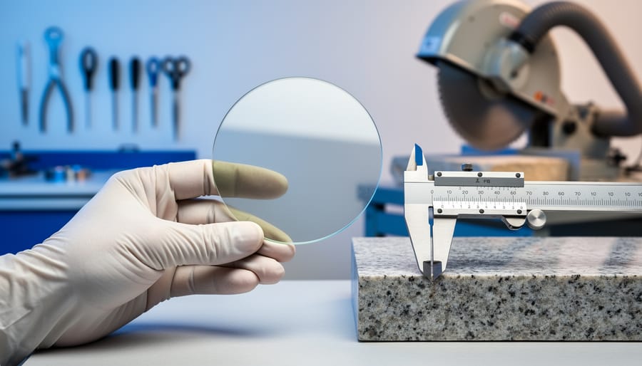
Slicing and Preparing Substrates
The precision required for slicing silicon ingots into wafers mirrors the exacting standards of high-end stone fabrication, though the scale differs dramatically. Silicon wafers measure just 775 micrometers thick with tolerances under 20 micrometers, while premium stone slabs typically range from 2-3 centimeters with tolerances of 1-2 millimeters. Both industries face the same fundamental challenge: extracting maximum value from expensive raw materials while minimizing waste.
| Aspect | Silicon Wafer Slicing | Stone Slab Cutting |
|---|---|---|
| Thickness Tolerance | ±20 micrometers | ±1-2 millimeters |
| Cutting Method | Diamond wire saws | Diamond wire or gang saws |
| Yield Target | 90-95% material recovery | 75-85% usable slabs |
| Quality Control | Laser scanning, automated inspection | Visual inspection, digital measurement |
This comparison reveals how advanced manufacturing processes share common principles despite serving vastly different markets. Diamond wire technology, originally developed for semiconductor applications, has revolutionized stone cutting by reducing kerf loss and enabling thinner slabs. The economics are compelling: improving yield by just 5% on a premium marble block worth $50,000 directly adds $2,500 to the bottom line.
Precision Patterning: Lithography Meets Stone Detailing
The Art of Subtractive Manufacturing
Whether you’re carving integrated circuits from silicon wafers or shaping granite for a luxury countertop, the fundamental challenge remains identical: how do you remove material without destroying what you’re creating?
In semiconductor fabrication, engineers use photolithography and chemical etching to carve away unwanted silicon, creating the microscopic pathways that will eventually conduct electricity. The tolerances are staggering, modern chips feature structures measuring just 3 nanometers across, roughly 30,000 times thinner than a human hair. A single misaligned cut or over-etched circuit can render millions of transistors useless.
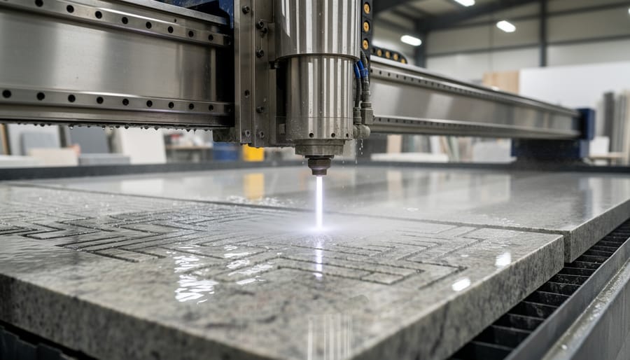
Stone fabricators face a similar precision challenge, albeit at a different scale. Precision stone cutting requires accounting for the material’s natural grain patterns, hardness variations, and hidden fractures that can propagate unexpectedly during cutting. A waterjet cutter operating at 60,000 PSI must maintain accuracy within fractions of a millimeter, especially when creating intricate inlays or matching book-matched slabs.
Both industries share an unforgiving reality: you can’t add material back once it’s removed. Semiconductor fabs combat this through multiple inspection stages and automated optical verification systems. Stone shops rely on experienced craftspeople who understand how different stones respond to cutting pressure, blade speed, and cooling water flow. The consequences of error differ in scale but not in principle, whether you’ve ruined a $10,000 silicon wafer or a rare marble slab, the material is permanently compromised.
Templates, Masks, and Repeatability
In semiconductor manufacturing, photomasks serve as the master templates that define circuit patterns on silicon wafers. These glass plates, etched with intricate designs measured in nanometers, enable manufacturers to reproduce identical chip layouts millions of times with absolute precision. The photomask acts as a stencil during photolithography, projecting its pattern onto light-sensitive material that coats the wafer surface.
Stone fabricators rely on a similar principle when creating multiple pieces from a single design. Templates, whether physical patterns made from thin plywood or digital files loaded into CNC machines, ensure that each countertop edge, each sink cutout, and each decorative inlay matches the original specification exactly. A fabricator cutting ten identical bathroom vanities doesn’t measure each piece individually; they create one accurate template and replicate it.
The value extends beyond simple reproduction. Templates capture accumulated knowledge and refinement. Just as semiconductor engineers spend months perfecting a photomask design to eliminate defects, stone fabricators develop templates that account for material behavior, tool characteristics, and installation requirements. A well-designed template for a curved granite bar top might include compensation for the slight flex in the stone during handling, or extra material at stress points.
Both industries understand that template quality directly impacts production efficiency and final product consistency.
Layering and Surface Treatment Techniques
In semiconductor fabrication, deposition processes add microscopically thin films of materials onto wafer surfaces with atomic-level precision. Chemical vapor deposition (CVD) introduces reactive gases that decompose and bond to the substrate, while physical vapor deposition (PVD) uses techniques like sputtering to transfer material particles from a target source. Each layer might measure just nanometers thick, yet manufacturers must control thickness uniformity, adhesion strength, and material properties across the entire wafer.
Stone finishing professionals employ remarkably similar principles when applying sealers and coatings to marble, granite, or quartzite. The substrate preparation mirrors semiconductor cleaning protocols: surfaces must be completely dry, free from contaminants, and properly textured for optimal adhesion. Penetrating sealers work through a process analogous to CVD, where carrier solvents transport active ingredients deep into the stone’s porous structure. As the solvent evaporates, protective compounds bond with the mineral matrix below the surface.
Topical coatings function more like PVD processes, building up protective films on the stone surface itself. Professional applicators control variables including ambient temperature, humidity levels, application pressure, and cure times. A single coating might measure only 50-100 microns thick, yet this layer must withstand daily wear, chemical exposure, and environmental stress.
The parallels extend to quality verification. Semiconductor manufacturers use ellipsometry to measure film thickness with angstrom-level accuracy. Stone professionals rely on water absorption tests, measuring contact angles and penetration rates to verify sealer effectiveness. Both industries recognize that rushed application leads to adhesion failures, uneven coverage, or premature degradation.
Multi-layer approaches appear in both fields too. Semiconductors often require dozens of different films stacked in precise sequences. High-performance stone installations might combine a penetrating sealer base layer with specialized topical coatings for enhanced stain resistance or slip prevention. The fundamental challenge remains identical: achieving uniform, durable layers that enhance the substrate’s performance without compromising its essential characteristics.
Cleanroom Standards vs. Fabrication Shop Hygiene
Why Contamination Control Matters at Any Scale
Contamination can destroy months of work in seconds, whether you’re fabricating a microchip or installing a marble countertop. In semiconductor facilities, a single airborne particle measuring just 0.5 microns, about 100 times smaller than a human hair, can short-circuit an entire wafer containing hundreds of chips worth millions of dollars. The industry loses billions annually to particle-induced defects that slip past quality controls.
Stone fabrication faces parallel challenges with different scales. A granite slab destined for a luxury hotel lobby can be ruined by metal shavings embedded during cutting, creating permanent rust stains that appear weeks after installation. Silica dust settling on a freshly honed surface creates microscopic scratches during polishing, turning what should be a mirror finish into a hazy disappointment. The rework costs are substantial, removing and replacing a compromised installation runs $15,000 to $50,000 depending on project scope.
The economic principle remains identical across both industries: prevention costs far less than correction. Semiconductor fabs invest heavily in HEPA filtration and cleanroom protocols because a $2 million contamination event justifies significant protective infrastructure. Stone fabricators increasingly adopt similar thinking, installing dust collection systems and implementing staging protocols that separate cutting operations from finishing areas. One contaminated batch teaches an expensive lesson about the value of controlled environments, regardless of what you’re manufacturing.
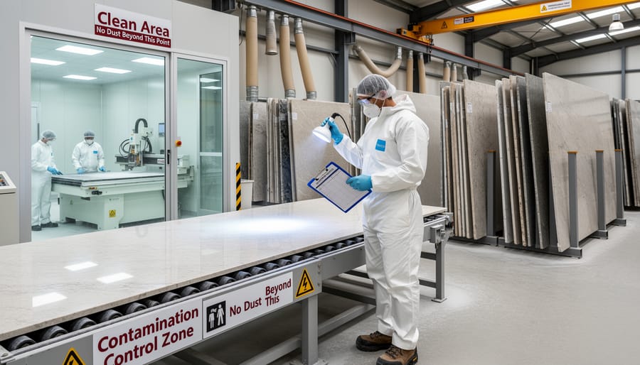
Practical Applications for Stone Professionals
Your stone workshop might not require a cleanroom, but semiconductor-grade thinking can transform your operations. Start with zone designation: create distinct areas for cutting, polishing, and final inspection. Dust migration between zones compromises finish quality just as particle contamination ruins microchips.
Implement a material handling protocol. Track each slab from receiving to installation with documentation matching semiconductor lot tracking. Record environmental conditions during critical processes, humidity affects adhesive curing, temperature influences epoxy set times. This data becomes invaluable when troubleshooting quality issues.
Borrow the semiconductor industry’s defect classification system. Categorize surface imperfections by severity: critical defects that require rework, major flaws customers might notice, and minor variations within tolerance. Train your team to identify defects at each production stage rather than discovering problems at final inspection.
Consider investing in basic metrology tools. Digital calipers and surface roughness testers cost a fraction of semiconductor equipment but provide objective quality metrics. Measure critical dimensions before and after polishing. Track tool wear patterns. These measurements reveal process drift before it affects finished products, preventing costly rework and customer complaints.
Quality Control and Inspection Technologies
The pursuit of zero defects drives innovation in both semiconductor fabrication and stone processing. In chip manufacturing, optical inspection systems scan wafers at nanometer resolution, detecting microscopic flaws that could compromise circuit performance. These automated systems analyze millions of data points per second, identifying contaminants, pattern irregularities, and surface defects invisible to the human eye.
Stone fabricators have adapted similar principles, though at vastly different scales. While a chip inspector searches for nanometer-level impurities, stone quality controllers examine slabs for structural fissures, color consistency, and surface uniformity. Digital imaging systems now map entire slabs, creating detailed profiles that reveal hidden weaknesses before cutting begins. This technology prevents costly mistakes and material waste.
| Technology | What It Detects | Semiconductor Application | Stone Fabrication Use |
|---|---|---|---|
| Optical Inspection | Surface defects, pattern errors | Wafer contamination, circuit flaws | Color variation, surface cracks |
| Electron Microscopy | Nanoscale structures, composition | Layer thickness, material purity | Crystal structure, mineral composition |
| Automated Imaging | Overall quality metrics | Die-level defect mapping | Full slab surface analysis |
| Spectroscopy | Chemical composition | Dopant concentration | Mineral identification, purity |
The way semiconductor manufacturing influences modern stone processing extends to non-destructive testing methods. Ultrasonic scanning, borrowed from semiconductor quality assurance, now helps detect internal voids in marble and granite without damaging the material. These systems send sound waves through the stone, mapping density variations that indicate structural weaknesses.
Machine learning algorithms further enhance inspection accuracy. Systems trained on thousands of samples can predict potential failure points, recommend optimal cutting patterns, and even suggest finishing techniques based on a stone’s unique characteristics. This intelligence reduces human error and improves consistency across production runs.
Lessons Stone Professionals Can Learn from Chip Manufacturing
The semiconductor industry’s obsession with perfection offers several practical lessons that stone fabricators can implement immediately.
Document Everything
Chip makers maintain meticulous records of every parameter, temperature, pressure, chemical concentrations, timing. Stone shops can adopt similar rigor by documenting blade specifications, water pressure settings, feed rates, and polishing sequences for each stone type. When you achieve a flawless finish on a challenging material, having exact parameters recorded means you can replicate that success consistently rather than relying on individual craftsman intuition.
Track Defects to Their Source
Semiconductor fabs don’t just count defective chips; they trace each flaw back to its origin in the process. Stone professionals can apply this same analytical approach. If you notice edge chipping on a particular granite, investigate systematically: Is it the blade type? Feed speed? Material support during cutting? This root-cause analysis prevents the same problem from recurring across multiple projects.
Measure Yield Like Revenue
In chip manufacturing, yield, the percentage of usable product, directly impacts profitability. Calculate your own yield metrics: How much material becomes unusable scrap? What percentage of slabs require rework? Where in your workflow do most problems occur? These numbers reveal where process optimization efforts will deliver the biggest returns.
Implement Incremental Improvements
Semiconductor companies don’t wait for revolutionary breakthroughs. They improve processes by tiny percentages continuously. Your shop can do the same. Maybe this month you focus on reducing saw blade changeover time by 10%. Next month, you work on minimizing water waste during polishing. Small gains compound into significant competitive advantages.
Create Process Standards
Develop written procedures for common operations. New employees shouldn’t need to figure out the best way to handle Calacatta marble through trial and error. Standardized processes ensure consistent quality regardless of who’s operating the equipment, and they create a foundation for identifying what actually needs improvement versus what’s just variation in technique.
Manufacturing excellence speaks a universal language that transcends industry boundaries. Whether engineers are etching silicon wafers or craftsmen are cutting granite slabs, the same fundamental principles govern success: unwavering respect for material quality, precision in every process step, relentless contamination control, and rigorous adherence to quality standards.
The semiconductor industry’s obsessive attention to detail offers valuable lessons for stone professionals. Clean room protocols remind us that environmental control matters, even when working with materials formed over millions of years. Multi-stage inspection processes demonstrate why quality checks at every phase prevent costly errors downstream. Standardized procedures ensure consistency that builds client trust and reduces waste.
Yet stone fabrication possesses advantages that silicon manufacturing can only envisage. Natural stone requires no energy-intensive purification or complex chemical processes. Each slab arrives with unique character already embedded by geological forces. Sustainability comes naturally when working with materials that have existed for millennia and will endure for centuries more.
The real opportunity lies in selective adoption. Implement semiconductor-inspired quality controls without losing the artisan touch that makes stone work special. Document processes with technical precision while celebrating the organic beauty that drew you to this craft. Balance modern manufacturing discipline with traditional material wisdom.
Cross-industry learning doesn’t dilute expertise. It sharpens it. When stone professionals embrace proven principles from advanced manufacturing while honoring their material’s natural excellence, they create work that satisfies both technical specifications and aesthetic aspirations.