Semiconductor manufacturing represents a cornerstone of modern technology, transforming raw silicon wafers into the powerful chips that drive everything from smartphones to advanced stone fabrication techniques in manufacturing facilities. This intricate process combines precision engineering, cutting-edge physics, and automated systems to create components at microscopic scales – often smaller than a human hair.
The journey from sand to semiconductor involves multiple sophisticated steps: photolithography etches precise circuit patterns, while ion implantation adds electrical properties to specific regions. Chemical vapor deposition builds microscopic layers atom by atom, creating the complex structures needed for modern integrated circuits. Quality control systems monitor every step, ensuring near-perfect precision in an industry where nanometer-scale accuracy determines success or failure.
As semiconductor technology continues advancing, it enables increasingly sophisticated automation and control systems across all manufacturing sectors. Understanding these processes isn’t just about appreciating technological achievement – it’s about recognizing how these innovations drive efficiency and precision in modern industrial applications, from basic electronics to advanced manufacturing equipment.
The Foundation of Modern Stone Cutting Technology
Silicon-Based Sensors in Stone Processing
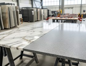
Modern stone processing relies heavily on semiconductor-based sensors to achieve unprecedented levels of accuracy and automation. These advanced sensors, integrated into precision cutting tools, enable real-time measurements of stone surfaces with accuracy down to fractions of a millimeter.
The sensors work by converting physical measurements into electronic signals, allowing automated systems to adjust cutting parameters instantly. This technology monitors blade positioning, cutting depth, and material density, ensuring consistent results across large stone slabs. For example, when cutting intricate countertop edges or complex architectural elements, these sensors detect variations in stone density and automatically adjust cutting speed and pressure.
Silicon-based sensors also play a crucial role in quality control, detecting microscopic flaws or irregularities that might be invisible to the human eye. This capability has revolutionized stone fabrication by reducing waste, improving efficiency, and enabling more complex designs that were previously impossible to execute consistently. The integration of these sensors has made stone processing more precise, safer, and more cost-effective than traditional manual methods.

Microprocessor Controls in Stone Equipment
Modern stone fabrication equipment relies heavily on advanced microprocessor controls powered by semiconductor technology. These sophisticated chips enable precise automation of cutting, polishing, and shaping processes that were once performed entirely by hand. Digital control systems now manage everything from water flow and blade speed to cutting depth and material positioning with unprecedented accuracy.
The integration of semiconductor-based controls has revolutionized stone processing by introducing features like automated tool path optimization, real-time monitoring of machine performance, and predictive maintenance alerts. CNC (Computer Numerical Control) machines, which form the backbone of modern stone fabrication, utilize multiple microprocessors to coordinate complex cutting patterns and maintain consistent quality across production runs.
These smart controls also enhance safety by automatically adjusting operating parameters based on material characteristics and monitoring system conditions. Advanced sensor systems, powered by specialized semiconductor chips, can detect potential issues before they become problems, helping to prevent equipment damage and reduce downtime. This technological evolution has significantly improved both the efficiency and precision of stone fabrication while reducing waste and operating costs.
Key Manufacturing Steps That Impact Tool Quality
Photolithography in Tool Production
Photolithography, a cornerstone of semiconductor manufacturing, has revolutionized the production of cutting tools used in stone fabrication. This precise technique uses light-sensitive materials and focused UV rays to create intricate patterns on silicon wafers, which ultimately translate into superior cutting components.
The process begins with a photoresist coating applied to the silicon substrate. Using advanced optical systems, manufacturers project specific patterns onto this coating through a photomask. Areas exposed to light undergo chemical changes, allowing for selective removal of material in subsequent steps. This level of precision, measured in nanometers, enables the creation of cutting edges and components with unprecedented accuracy.
For the stone industry, this technology has enabled the development of more efficient diamond cutting tools and precision-guided systems. The microscopic patterns created through photolithography help optimize the positioning and distribution of diamond particles in cutting segments, resulting in smoother cuts and reduced material waste.
Modern CNC machines and automated cutting systems benefit from semiconductor components manufactured through this process, offering enhanced control and monitoring capabilities. The integration of these high-precision elements has led to improved tool longevity, more consistent cutting performance, and better overall fabrication results.
This advanced manufacturing technique continues to push the boundaries of what’s possible in stone processing equipment, enabling fabricators to achieve increasingly precise and efficient results.

Chemical Vapor Deposition
Chemical Vapor Deposition (CVD) plays a crucial role in enhancing the durability and performance of stone processing tools. This advanced manufacturing process deposits thin films of hard materials, such as diamond or titanium nitride, onto cutting tools and abrasive equipment used in stone fabrication.
During the CVD process, precursor gases are introduced into a heated chamber where they react or decompose on the tool’s surface, forming a uniform protective coating. These coatings significantly extend tool life by providing exceptional wear resistance, reducing friction, and improving heat dissipation during stone cutting and polishing operations.
For example, diamond-coated cutting tools created through CVD technology can maintain their sharp edges up to five times longer than conventional tools when processing hard stones like granite. The process also allows for precise control over coating thickness and composition, ensuring optimal performance for specific stone applications.
The benefits of CVD coatings in stone processing include:
– Increased tool lifespan
– Improved cutting precision
– Reduced maintenance costs
– Enhanced surface finish quality
– Better heat resistance during operation
This technology has revolutionized stone fabrication by enabling faster processing speeds while maintaining exceptional quality standards. As the semiconductor industry continues to advance CVD techniques, stone processing tools become increasingly sophisticated and efficient.
Etching and Surface Treatment
Etching and surface treatment processes play a crucial role in semiconductor manufacturing, directly impacting the performance and longevity of cutting tools used in stone fabrication. During this stage, precise chemical or plasma-based techniques remove specific material layers to create intricate patterns and structures on the semiconductor surface.
The process typically involves two main approaches: wet etching, which uses liquid chemical solutions, and dry etching, which employs plasma or ion bombardment. These techniques are carefully controlled to achieve exact depth and pattern specifications, often working at the microscopic level to create features as small as a few nanometers.
Modern stone cutting tools benefit from semiconductor manufacturing principles through enhanced surface treatments. These treatments create wear-resistant coatings and optimize blade edges for improved cutting precision. The application of semiconductor etching techniques allows for the development of specialized tool surfaces that resist corrosion, reduce friction, and maintain sharper edges for longer periods.
The precision achieved through semiconductor etching processes has revolutionized tool manufacturing, resulting in cutting implements that maintain their edge integrity significantly longer than traditional tools. This translates to reduced maintenance requirements, more consistent cutting quality, and improved overall efficiency in stone fabrication operations.
For fabricators, this means fewer tool replacements, more precise cuts, and ultimately, better final products for their clients.
Benefits for Stone Fabrication Industry
Enhanced Precision and Efficiency
The integration of semiconductor technology in stone fabrication equipment has revolutionized precision and efficiency in manufacturing processes. Modern CNC machines now achieve cutting accuracies within 0.1 millimeters, thanks to advanced semiconductor-based sensors and control systems. This level of precision ensures consistent quality across large production runs and minimizes material waste.
These improvements are particularly evident in the processing speed of contemporary equipment. What once took hours can now be completed in minutes, with automated systems capable of maintaining high accuracy even at increased cutting speeds. For example, advanced bridge saws equipped with semiconductor-controlled motors can process complex stone cuts up to 40% faster than traditional equipment while maintaining superior edge quality.
The enhanced precision also extends to surface finishing operations. Automated polishing systems utilize semiconductor-based feedback mechanisms to adjust pressure and speed in real-time, ensuring uniform finish quality across varied stone surfaces. This technology adapts to different material densities and compositions, preventing over-polishing or surface damage.
Quality control has also been transformed through semiconductor-enabled vision systems that can detect microscopic flaws and variations in stone surfaces. These systems perform rapid inspections during production, allowing immediate adjustments to maintain optimal cutting parameters and ensure consistent results throughout the manufacturing process.

Cost and Waste Reduction
The integration of semiconductor-enhanced tools in manufacturing processes has revolutionized cost management and waste reduction in the industry. Advanced semiconductor sensors and controls enable precise material usage, significantly reducing waste compared to traditional methods. These systems can detect and adjust for variations in material thickness, cutting speed, and tool wear in real-time, ensuring optimal resource utilization.
Manufacturing facilities implementing semiconductor-based automation systems report an average reduction in material waste of 15-20%. This improvement directly translates to substantial cost savings, particularly when working with expensive materials. The technology’s ability to maintain consistent quality while minimizing errors reduces the need for rework and replacement parts.
Smart monitoring systems powered by semiconductor technology track energy consumption patterns and identify opportunities for optimization. Many facilities have achieved energy savings of up to 30% by implementing these solutions. Additionally, predictive maintenance capabilities help prevent unexpected equipment failures, reducing downtime and associated costs.
The environmental impact is equally significant. Reduced material waste means less landfill contribution, while improved energy efficiency leads to a smaller carbon footprint. Companies using semiconductor-enhanced manufacturing processes often report meeting sustainability goals more effectively while maintaining high production standards.
These advancements have made semiconductor technology a crucial investment for manufacturers looking to balance economic efficiency with environmental responsibility. The initial implementation costs are typically offset within 2-3 years through reduced operational expenses and improved resource management.
Future Developments and Industry Impact
The semiconductor manufacturing industry continues to evolve rapidly, bringing significant advancements to stone processing technology. As chip manufacturing techniques become more sophisticated, we’re seeing the emergence of smarter, more precise stone fabrication equipment that can deliver unprecedented levels of accuracy and efficiency.
One of the most promising developments is the integration of artificial intelligence and machine learning capabilities, made possible by advanced semiconductor components. These systems can analyze stone patterns, optimize cutting paths, and automatically adjust processing parameters in real-time, resulting in reduced waste and improved product quality.
The miniaturization of semiconductor components is enabling the development of more compact and energy-efficient stone processing equipment. This trend is particularly beneficial for smaller fabrication shops, making advanced technology more accessible and cost-effective for businesses of all sizes.
Looking ahead, experts predict that quantum computing applications in semiconductor manufacturing will revolutionize stone processing optimization. These developments could lead to ultra-precise cutting algorithms and enhanced material analysis capabilities, potentially transforming how we approach complex stone fabrication projects.
The industry is also seeing innovations in sensor technology, with new semiconductor-based systems capable of detecting microscopic flaws and variations in stone materials before processing begins. This advancement helps prevent costly mistakes and ensures consistent quality throughout the manufacturing process.
Environmental considerations are driving the development of more energy-efficient semiconductor components, which in turn leads to greener stone processing equipment. Manufacturers are focusing on reducing power consumption while maintaining or improving performance, addressing both environmental concerns and operational costs.
As these technologies continue to mature, we can expect to see more automated and integrated stone processing solutions that combine multiple functions into single, efficient systems. This evolution will likely reshape the stone fabrication industry, making high-quality stone products more accessible while reducing production times and costs.
The semiconductor manufacturing process continues to evolve rapidly, pushing the boundaries of what’s possible in modern technology. As we’ve explored throughout this article, this sophisticated process combines precision engineering, advanced materials science, and cutting-edge technology to create the microchips that power our digital world.
The industry faces both exciting opportunities and significant challenges ahead. The ongoing drive toward smaller transistors and more efficient chips has led to innovations in photolithography, materials development, and quality control methods. As demand for semiconductors grows across various sectors, including automotive, consumer electronics, and industrial applications, manufacturers are investing heavily in expanding production capacity and developing new technologies.
Looking forward, emerging technologies like extreme ultraviolet lithography (EUV) and advanced packaging techniques promise to unlock new possibilities in chip design and performance. The industry is also focusing on sustainability, with increasing emphasis on reducing energy consumption and minimizing environmental impact during manufacturing.
Despite challenges such as supply chain complexities and the need for massive capital investment, the semiconductor manufacturing process remains crucial to technological advancement. As we move toward an increasingly connected world, the continued refinement and innovation in semiconductor manufacturing will play a vital role in shaping our technological future.