Nature engineered the world’s first photonic crystals millions of years ago, long before scientists understood the physics behind their mesmerizing optical effects. The iridescent flash of an opal, the shimmering wings of a morpho butterfly, and the brilliant colors of certain beetles all demonstrate nature’s mastery of manipulating light through precisely ordered nanostructures. These natural photonic crystals control light not through pigments or dyes, but through periodic variations in structure at scales comparable to light wavelengths—typically hundreds of nanometers.
Photonic crystals function as optical semiconductors, creating “photonic band gaps” that prohibit certain wavelengths of light from propagating while allowing others to pass freely. This selective control over light makes them invaluable for applications ranging from optical computing and telecommunications to advanced sensors and solar energy harvesting. The same structural principles that create opal’s play-of-color now inspire cutting-edge technologies in fiber optics, laser design, and LED efficiency improvements.
Understanding photonic crystals bridges two worlds: the ancient geological processes that created precious opal deposits and the frontier of modern optoelectronics. Australian precious opal remains the gold standard for natural photonic crystals, with its regular arrays of silica spheres creating spectral displays that engineers strive to replicate synthetically. The formation process, requiring millions of years of precise conditions, produces optical properties that reveal fundamental principles of light-matter interaction.
This intersection of natural stone and advanced physics demonstrates how traditional materials continue to inform innovation. For architects, designers, and material scientists, photonic crystals represent both aesthetic inspiration and functional technology—a dual value proposition that positions natural stone at the forefront of biomimetic design and photonic engineering.
What Are Photonic Crystals? Nature’s Light Architecture
The Science Behind the Shimmer
The mesmerizing play of color in certain natural stones isn’t created by pigments or dyes, but rather by their internal architecture at the nanoscale. This phenomenon, known as structural color, occurs when light interacts with periodic nanostructures—regularly repeating patterns that are smaller than the wavelength of visible light.
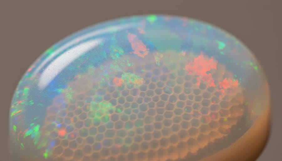
Opal provides the perfect natural example of this principle in action. Within precious opal, microscopic silica spheres arrange themselves in ordered, three-dimensional arrays with remarkable precision. These spheres, typically between 150 and 400 nanometers in diameter, stack together in a formation similar to oranges in a crate. The spaces between these spheres create a periodic structure that acts as a natural photonic crystal.
When white light enters an opal, it encounters this orderly lattice. The regular spacing causes specific wavelengths to reflect back while others pass through or are absorbed. This selective reflection, called Bragg diffraction, produces the brilliant flashes of color that make opal so captivating. As you tilt the stone, different angles reveal different colors because the light interacts with various planes within the crystal structure.
The specific colors displayed depend on the size of the silica spheres and their arrangement. Smaller spheres produce blues and greens, while larger spheres generate reds and oranges. This natural engineering demonstrates how precise structural organization at the nanoscale can manipulate light without any chemical colorants—a principle that scientists now replicate in synthetic photonic materials for advanced technological applications.
Why Natural Stone Matters in This Field
Nature perfected photonic crystals long before humans entered the laboratory. Precious opal, formed over millions of years through the orderly stacking of silica spheres, represents Earth’s most stunning example of natural photonic architecture. These microscopic structures diffract light into brilliant spectral displays, creating the gemstone’s signature play-of-color without any pigmentation whatsoever.
This natural phenomenon has become a blueprint for modern technology. Scientists and engineers study opal’s nanoscale geometry to design synthetic photonic crystals for telecommunications, optical computing, and advanced sensors. The stone’s ability to manipulate light through purely structural means—rather than chemical absorption—demonstrates principles that researchers now replicate in materials ranging from polymer films to semiconductor devices.
Understanding opal’s photonic properties bridges aesthetics and innovation. The same mechanisms that make opal captivating in jewelry inspire breakthroughs in fiber optics, anti-counterfeiting technologies, and energy-efficient coatings. For designers and architects, this connection offers fresh perspective on natural stone as more than decorative material—it’s a sophisticated optical system millions of years in development, offering both visual beauty and technological insight that continues shaping how we engineer light-manipulating materials today.
Opal: Nature’s Original Photonic Crystal
The Microscopic Structure That Creates Play-of-Color
At the heart of opal’s mesmerizing play-of-color lies an incredibly precise natural architecture. The secret is in how tiny silica spheres, each measuring between 150 and 400 nanometers in diameter, organize themselves into remarkably uniform, three-dimensional grids. To visualize this, imagine stacking oranges at a fruit stand: when arranged carefully, they naturally settle into a repeating pattern where each orange nestles into the gaps created by the layer below. Opal’s silica spheres do exactly this, but at a scale 10,000 times smaller than a human hair.
This ordered arrangement transforms opal into what scientists call a photonic crystal—a material whose structure directly controls how light behaves within it. When white light enters the stone, it encounters this regular lattice of silica spheres separated by water or air. The spacing between spheres is comparable to the wavelengths of visible light, causing specific colors to be reinforced while others are suppressed through a process called constructive and destructive interference.
Think of it like waves in a swimming pool bouncing off walls at precise intervals. When the timing is just right, waves amplify each other; when it’s off, they cancel out. In opal, light waves reflecting from different layers of silica spheres interact in exactly this way. The particular color you see depends on the sphere size, their spacing, and the viewing angle—which explains why opal’s colors shift dramatically as you rotate the stone.
This natural phenomenon occurs without any pigments or dyes. The color is purely structural, created by geometry and physics working in perfect harmony at the nanoscale.
From Australian Mines to Research Labs
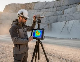
Australian opal mines, particularly those in regions like Coober Pedy and Lightning Ridge, have become unexpected sources of inspiration for cutting-edge materials research. Scientists regularly collect opal samples from these deposits to study the precise structural arrangements that create their signature color play. Using advanced imaging techniques including electron microscopy and X-ray crystallography, researchers can map the three-dimensional arrangement of silica spheres within precious opal at nanometer scales.
This analysis reveals how sphere size, uniformity, and packing patterns determine which wavelengths of light get reflected or blocked, creating the specific colors we observe. By understanding these natural blueprints, materials scientists can replicate and even improve upon nature’s design. Research laboratories worldwide maintain collections of Australian opal specimens as reference materials for developing synthetic photonic crystals.
The insights gained from studying natural opal have accelerated the development of artificial photonic crystals for telecommunications, optical computing, and sensor technologies. Scientists have learned that the most vibrant opals possess remarkably uniform sphere sizes with variations of less than five percent, a level of precision they now aim to achieve in manufactured materials.
Modern fabrication techniques, including self-assembly methods inspired by opal formation processes, allow researchers to create photonic crystals tailored for specific applications. These synthetic materials can be designed to manipulate light at wavelengths impossible in natural opal, extending beyond visible light into infrared and ultraviolet ranges critical for advanced technologies.
From Stone to Silicon: Modern Applications of Photonic Crystals
Fiber Optics and Telecommunications
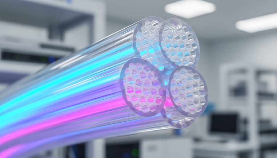
The naturally occurring photonic crystal structure found in precious opal has inspired revolutionary advances in fiber optic telecommunications. Engineers have developed synthetic photonic crystal fibers that manipulate light with unprecedented precision, dramatically improving data transmission speeds and signal quality across networks worldwide.
These engineered fibers feature microscopic air holes arranged in patterns that mirror opal’s natural silica sphere arrangement. This structure allows telecommunications companies to guide light through optical cables with minimal signal loss, enabling faster internet speeds and more reliable long-distance communication. Photonic crystal fibers can transmit multiple wavelengths of light simultaneously without interference, effectively multiplying network capacity.
In signal processing applications, photonic crystals act as highly selective filters, isolating specific wavelengths for routing data through complex telecommunications systems. This wavelength selectivity reduces cross-talk between channels and improves overall network efficiency. Modern data centers increasingly rely on photonic crystal components to manage the massive information flows that power cloud computing and streaming services.
The technology has also enabled compact optical switches that redirect light signals without converting them to electrical signals, reducing energy consumption and processing delays. As telecommunications infrastructure evolves toward all-optical networks, photonic crystals inspired by natural stone continue driving innovation in how we transmit and process information globally.
LED Technology and Display Innovation
The study of photonic crystals in natural opals has revolutionized LED and display technology, offering more efficient and vibrant lighting solutions. Engineers have developed synthetic photonic structures that mimic opal’s periodic nanostructure to create LEDs with dramatically improved light extraction efficiency. Traditional LEDs lose significant light energy to internal reflection, but photonic crystal patterns etched onto LED surfaces allow more photons to escape, increasing brightness while reducing energy consumption.
In display technology, photonic crystal principles have inspired new screen designs that enhance color purity and viewing angles. Some manufacturers now incorporate photonic layers that manipulate light wavelengths more precisely than conventional filters, producing richer colors with less backlight power. These biomimetic approaches, borrowed directly from natural stone structures, represent a sustainable innovation pathway where nature’s billions of years of optical engineering inform human technology.
Research continues into flexible photonic crystal displays and tunable color systems that could transform everything from smartphone screens to architectural lighting. By understanding how microscopic silica spheres in opal create such remarkable optical effects, scientists are developing next-generation devices that combine energy efficiency with superior visual performance, proving that ancient geological formations hold keys to modern technological challenges.
Solar Energy and Light Harvesting
Photonic crystals offer transformative potential for solar energy applications by manipulating light at the nanoscale to maximize absorption and energy conversion. When integrated into solar panel designs, these periodic nanostructures can redirect light that would otherwise be reflected or pass through, effectively trapping photons within the photovoltaic material. This light-trapping mechanism significantly increases the optical path length, allowing thinner solar cells to capture more energy while reducing material costs.
Engineers are developing anti-reflective coatings based on photonic crystal principles that minimize energy loss from surface reflection, boosting overall panel efficiency by 5-10%. Some designs incorporate inverse opal structures—inspired by natural gemstones—that selectively filter and concentrate specific wavelengths optimal for energy conversion. These biomimetic approaches connect ancient geological formations with modern sustainable energy solutions.
Advanced photonic crystal configurations also enable wavelength-selective absorption, converting otherwise wasted infrared and ultraviolet radiation into usable electricity. As manufacturing techniques improve, these nature-inspired light management systems promise to make solar technology more efficient, affordable, and accessible for widespread adoption in residential and commercial applications.
Medical Devices and Biosensors
Photonic crystal principles are revolutionizing healthcare technology through advanced biosensors and medical devices. These nanostructured materials enable label-free detection of biomarkers, viruses, and pathogens with unprecedented sensitivity. Wearable health monitors now incorporate photonic crystal sensors for non-invasive glucose monitoring and early disease detection. The same structural color principles found in opal—nature’s photonic crystal—inspire these innovations. As research progresses, connections between bio-inspired designs and natural stone sensors suggest promising applications where traditional materials meet cutting-edge diagnostic technology, potentially transforming both medical devices and smart building health monitoring systems.
Natural Stone in Contemporary Photonic Design
Opal in High-End Architectural Applications
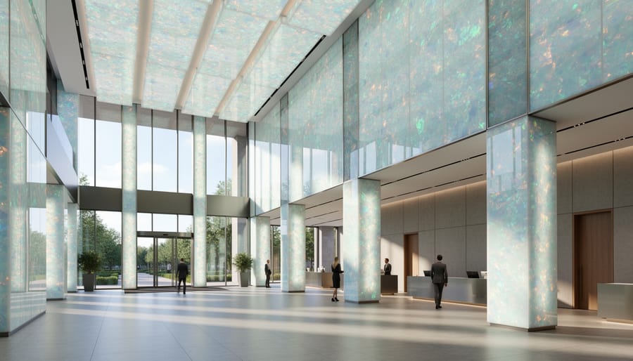
Precious opal has emerged as a captivating material choice in high-end architectural applications, where designers and architects seek to merge natural beauty with scientific intrigue. The stone’s unique photonic crystal structure creates dynamic color displays that transform with lighting conditions and viewing angles, making each installation a living work of art.
In luxury residential projects, Australian precious opal has been incorporated into feature walls, backlit panels, and custom furniture pieces. One notable example includes a private residence in Dubai where thin opal slices were embedded in translucent resin panels, creating a luminous room divider that shifts from fiery reds to electric blues throughout the day. The installation serves both as a stunning visual centerpiece and a conversation starter about natural photonic phenomena.
Commercial spaces have also embraced opal’s optical properties. A boutique hotel in Sydney features an opal-inlaid reception desk that captures attention with its play-of-color, while a high-end jewelry store in New York utilizes backlit opal panels in display cases to create an ethereal shopping environment. These applications demonstrate how opal’s natural photonic structure can enhance brand identity and create memorable customer experiences.
The integration of opal into smart building applications represents an exciting frontier, where its optical properties could potentially be combined with lighting systems and sensors to create responsive architectural elements. As architects continue exploring biomimetic design principles, opal stands as a prime example of nature’s engineering excellence translated into functional luxury.
Educational and Exhibition Spaces
Museums and science centers worldwide have recognized the educational value of natural photonic crystals, particularly opals, as powerful teaching tools that bridge mineralogy, physics, and materials science. The Smithsonian National Museum of Natural History prominently features precious opals in its geology exhibit, where interactive displays explain how their ordered silica sphere structure creates the play-of-color phenomenon through light diffraction. Visitors can observe how rotating specimens under different lighting conditions demonstrates the principles of structural coloration versus pigment-based color.
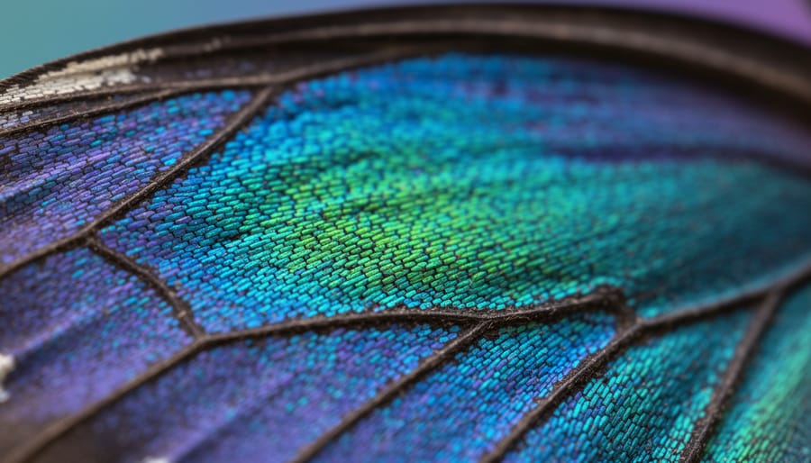
The California Academy of Sciences incorporates Australian boulder opals into its “Color of Life” exhibit, using them to illustrate how nature engineers light manipulation at the nanoscale. These specimens serve alongside butterfly wings and peacock feathers to demonstrate convergent evolution of photonic structures across different domains. Educational signage explains the direct correlation between sphere size and color wavelengths, making complex optical physics tangible for students.
University geology departments increasingly use opal specimens as laboratory teaching aids. Students at MIT and Stanford examine thin sections under electron microscopy to visualize the regular lattice arrangements responsible for photonic properties. These hands-on experiences help students understand both crystallography fundamentals and advanced concepts in photonics research.
Architectural schools have also embraced these materials. Design studios feature opal samples alongside synthetic photonic crystals, challenging students to envision biomimetic applications where natural stone inspires technological innovation. This interdisciplinary approach demonstrates how ancient geological processes continue informing cutting-edge materials development, making natural photonic crystals invaluable educational assets across multiple scientific and design disciplines.
The Future: Biomimetic Materials Inspired by Stone
Lab-Grown Photonic Crystals vs. Natural Stone
Scientists have successfully synthesized photonic crystals in laboratories, but these engineered materials differ significantly from natural stones like opal. Lab-grown photonic crystals offer precise control over structure, allowing researchers to fine-tune optical properties for specific applications like optical computing, sensors, and telecommunications. They can be manufactured with uniform patterns and predictable performance, making them ideal for industrial applications requiring consistency.
Natural opals, however, possess unique characteristics that remain challenging to replicate. Their irregular silica sphere arrangements create distinctive color play and variation that gives each stone individual character. This natural imperfection contributes to their aesthetic appeal and value in jewelry and decorative applications. Natural stones also demonstrate remarkable durability, having maintained their photonic structures over millions of years.
The distinction between synthetic and natural materials extends to evaluation methods. Modern advanced material characterization techniques help identify and authenticate natural photonic crystals while guiding synthetic production.
Both materials serve valuable purposes: lab-grown crystals excel in technological applications requiring precision, while natural stones remain unmatched in aesthetic applications where uniqueness and geological authenticity matter most to designers and consumers.
Sustainability and Material Science
Nature’s photonic crystals, particularly those found in precious opal, offer valuable blueprints for developing more sustainable technological solutions. By studying how these natural structures manipulate light without relying on chemical pigments or energy-intensive processes, scientists and engineers can design eco-friendly alternatives to conventional materials. Natural stone’s photonic properties demonstrate that stunning optical effects can be achieved through physical structure alone, inspiring innovations in everything from energy-efficient building materials to low-impact display technologies.
The lessons learned from opal’s nanostructure have influenced advances in synthetic material manufacturing, where researchers replicate these naturally occurring patterns to create materials with enhanced optical properties while minimizing environmental impact. These biomimetic approaches reduce the need for toxic dyes and energy-intensive manufacturing processes. Additionally, understanding how natural photonic crystals form over geological timescales helps scientists develop more durable, longer-lasting materials that require less frequent replacement, further contributing to sustainability goals. As industries seek greener alternatives, natural stone’s photonic properties continue to inform the development of technologies that balance performance with environmental responsibility.
The remarkable journey from ancient opal formations to cutting-edge photonic devices reveals a profound truth: nature has been engineering sophisticated optical technologies for millions of years. These natural photonic crystals, formed through gradual geological processes, continue to offer invaluable blueprints for scientists and engineers developing the next generation of optical computing, telecommunications, and sensing technologies. The regular nanostructure that creates opal’s characteristic play-of-color is the same fundamental architecture that researchers are painstakingly recreating in laboratories worldwide, demonstrating that natural stone’s significance extends far beyond its traditional decorative and architectural applications.
For architects, designers, and consumers, this connection between natural materials and advanced technology opens new perspectives on the stones we incorporate into our spaces. When you select opal or other structurally colored materials, you’re not just choosing aesthetic beauty—you’re bringing a piece of nature’s engineering mastery into your environment. This intersection of ancient formation and modern innovation reminds us that natural stone remains relevant in our technological age, serving simultaneously as inspiration, teaching tool, and functional material.
We encourage you to view natural stone through this broader lens, recognizing its role as both timeless building material and catalyst for scientific advancement. Whether you’re specifying materials for a project or simply appreciating natural stone’s beauty, consider the extraordinary nanoscale architecture that took millennia to perfect—and continues to shape our technological future today.