Precision manufacturing transforms raw materials into intricate products through methodical, controlled processes. The semiconductor industry exemplifies this principle at its most extreme: producing microchips requires tolerances measured in nanometers, cleanroom environments thousands of times purer than hospital operating rooms, and multi-billion dollar facilities. Yet the fundamental concepts behind semiconductor fabrication offer surprising relevance for anyone working with precision materials, including natural stone professionals seeking to refine their craft.
Semiconductor manufacturing begins with ultra-pure silicon wafers that undergo dozens of processing steps, each demanding absolute precision. Photolithography projects circuit patterns onto wafer surfaces using light wavelengths smaller than visible spectrum. Chemical etching removes unwanted material with accuracy measured in atomic layers. Deposition techniques build up thin films of various materials, creating the three-dimensional structures that form transistors and interconnects.
The parallels to stone processing become clear when examining the core principles. Both industries demand meticulous surface preparation, where microscopic imperfections compromise final quality. Temperature control proves critical in both semiconductor diffusion furnaces and stone resin curing processes. Quality inspection occurs at multiple stages, rejecting defective materials before they advance through expensive subsequent steps.
Process contamination presents challenges across both sectors. Semiconductor fabs invest heavily in particulate control because a single dust speck can destroy an entire chip. Stone fabricators face analogous concerns: residual dust affects adhesive bonding, foreign particles create weak points in composite materials, and surface contaminants prevent proper sealing.
Understanding semiconductor manufacturing principles illuminates broader truths about precision production. The same attention to environmental control, process standardization, and defect prevention that enables modern electronics manufacturing translates directly to achieving consistent, high-quality results in natural stone fabrication and installation.
The Raw Material Selection Process: Silicon and Stone
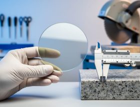
Both semiconductor fabrication and stone processing begin with a critical decision that determines every downstream outcome: selecting raw material that meets exacting standards. Silicon wafer manufacturers inspect crystalline structure, doping uniformity, and surface flatness down to nanometer tolerances. Stone fabricators evaluate mineral composition, vein patterns, and structural soundness across entire slabs. The parallels run deeper than you might expect.
Semiconductor-grade silicon wafer manufacturing demands 99.9999999% purity, what the industry calls “nine nines.” A single impurity atom per billion can create electrical defects that render entire chips useless. Stone selection operates on different scales but follows similar logic. Granite containing excessive mica may delaminate under stress. Marble with hidden microfractures fails during installation. Both industries have learned that ignoring material characteristics upfront costs far more than careful initial selection.
Quality grading systems in each field reflect this reality. Semiconductor wafers receive ratings based on crystal orientation, oxygen content, and defect density measured by automated scanners. Natural stone gets classified by appearance grades, but serious fabricators go further, testing absorption rates, flexural strength, and freeze-thaw resistance. The best stone fabrication techniques mean nothing if the base material lacks the necessary properties for the application.
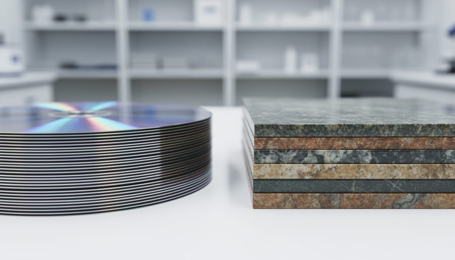
| Assessment Factor | Semiconductor Silicon | Natural Stone |
|---|---|---|
| Purity/Consistency | 99.9999999% pure silicon; controlled dopant distribution | Mineral composition consistency; color uniformity across slab |
| Structural Defects | Crystal dislocations, slip lines measured at atomic scale | Fissures, voids, weak planes detected via visual and ultrasonic inspection |
| Grading System | Prime, test, monitor grades based on defect density per cm² | Premium, standard, commercial grades based on appearance and structural integrity |
| Sourcing Considerations | Single-crystal growth methods; vendor certification requirements | Quarry location, block selection, slab orientation relative to bedding planes |
Traceability matters in both industries. Semiconductor fabs track wafer lots back to specific ingot growth runs, documenting every thermal cycle. Stone fabricators increasingly document slab origins, recording quarry coordinates and block numbers. This allows them to source matching material for future phases and identify patterns when problems emerge. A consistent material selection process, backed by verifiable documentation, separates professional operations from those gambling on every job.
Precision Cutting and Shaping Techniques
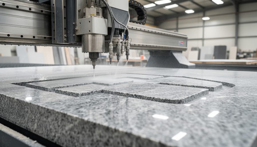
Layer-by-Layer Material Removal
In semiconductor manufacturing, etching removes material atom by atom through controlled chemical or plasma reactions. Engineers might strip away 50 nanometers of silicon dioxide in one step, then 30 nanometers of polysilicon in the next, building complex three-dimensional structures through dozens of sequential removal stages. Each layer comes off with tolerances measured in angstroms, ten-billionths of a meter.
Stone fabrication follows the same principle at a different scale. When transforming rough granite into a polished countertop, fabricators work through progressively finer grits: 50-grit removes saw marks and major imperfections, 100-grit smooths the surface, 200-grit begins developing sheen. Each pass strips a thin layer, typically 0.5 to 1 millimeter total across the entire sequence. Rush through the progression, and you get burn marks or uneven surfaces. Skip a grit level, and scratches from the coarser abrasive remain visible.
Both processes demand patience and precision. Semiconductor engineers monitor etch depth with laser interferometry between each step. Stone professionals check their work by feel and visual inspection, adjusting pressure and dwell time based on how the surface responds. The granite slab and the silicon wafer share a fundamental requirement: each layer must come off cleanly before the next stage begins, or defects compound through subsequent steps and ruin the final product.
Template-Based Replication
In semiconductor fabrication, photomasks serve as the master blueprints that transfer intricate circuit patterns onto silicon wafers. These glass plates, coated with chrome patterns, act like industrial-scale stencils. When ultraviolet light shines through them during the photolithography process, they project exact circuit designs onto photosensitive material coating the wafer. A single mask might be reused thousands of times to create identical chips, and modern photolithography enables nanometer-scale precision that far exceeds what human hands could achieve.
Natural stone fabrication employs remarkably similar template-based methods. When producing architectural elements like balustrades, window surrounds, or decorative medallions that repeat throughout a building, fabricators create master templates from materials like plywood, acrylic, or aluminum. These templates guide CNC routers or manual cutting tools to reproduce identical profiles across dozens or hundreds of stone pieces. The principle mirrors semiconductor manufacturing: create one perfect master, then replicate it with minimal variation.
The benefits translate directly across industries. Templates eliminate cumulative errors that creep in when craftspeople measure and mark each piece individually. They ensure that the fortieth column capital matches the first, maintaining visual consistency crucial for large installations. For high-volume production runs, templates dramatically reduce labor time and material waste by standardizing the cutting path. The semiconductor industry’s obsessive focus on template accuracy and version control offers stone fabricators a proven framework for managing their own template libraries and ensuring that reproductions remain faithful to approved designs.
Quality Control and Defect Management
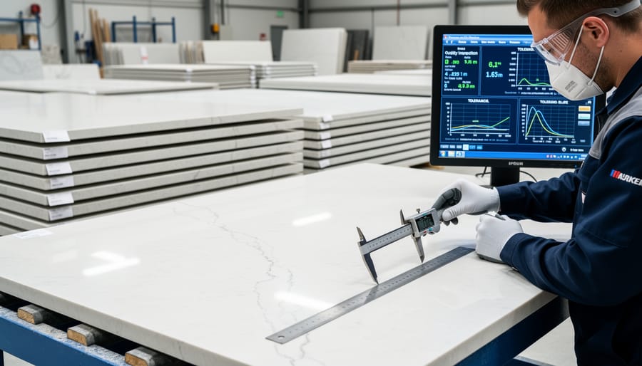
Semiconductor fabs inspect every wafer at multiple production stages, using automated optical systems that detect defects measuring mere nanometers. Stone fabricators have borrowed this multi-checkpoint philosophy, inspecting slabs upon arrival, after cutting, following surface treatment, and before installation. Both industries recognize that catching defects early prevents compounding errors and wasted resources downstream.
The semiconductor industry classifies defects with surgical precision: particles, scratches, pattern misalignments, and material inconsistencies each receive specific codes and severity ratings. Natural stone processing has developed parallel classification systems that categorize fissures, pitting, color variations, and structural weaknesses. This standardized approach allows fabricators to make consistent accept-or-reject decisions rather than relying on subjective judgment, directly improving the essential manufacturing processes that determine final product quality.
Both industries employ remarkably similar quality control techniques:
- Visual inspection protocols using controlled lighting to reveal surface anomalies
- Dimensional verification with laser measurement systems and coordinate measuring machines
- Surface analysis examining flatness, finish consistency, and reflectivity
- Defect mapping that documents flaw locations for process improvement analysis
- Batch tracking linking materials to specific production runs for traceability
Advanced stone fabricators now use digital imaging systems that photograph each slab, creating permanent records that track defects from quarry to installation. This mirrors semiconductor wafer mapping, where every imperfection’s coordinates are logged in databases. When patterns emerge, engineers trace problems to specific equipment, operators, or raw material batches.
The rejection criteria differ in scale but not philosophy. A semiconductor wafer with defects exceeding density thresholds gets scrapped, just as stone slabs with excessive fissuring or weak zones cannot proceed to fabrication. Both industries calculate yield rates, the percentage of acceptable product from raw material input, and use this metric to drive continuous improvement. Premium fabrication shops targeting architectural projects have adopted strict acceptance standards that would seem familiar to any chip manufacturer, recognizing that rigorous quality control protects reputation and reduces costly field failures.
Environmental Controls in Manufacturing
Walk into a semiconductor fab and you’ll immediately notice something unusual: the air pressure pushes outward when doors open, workers wear full-body suits, and not a speck of dust is visible. These facilities maintain cleanroom standards rated ISO Class 1 to 5, where particle counts are measured per cubic meter and even a single airborne contaminant can ruin an entire batch of chips worth millions.
The extreme environmental controls exist because semiconductor features measure just nanometers across. A particle invisible to the naked eye becomes a canyon-sized obstacle when you’re working at that scale. Temperature holds steady within 0.5 degrees Celsius, humidity stays controlled between 30-50 percent, and specialized filtration systems cycle the entire room’s air dozens of times per hour.
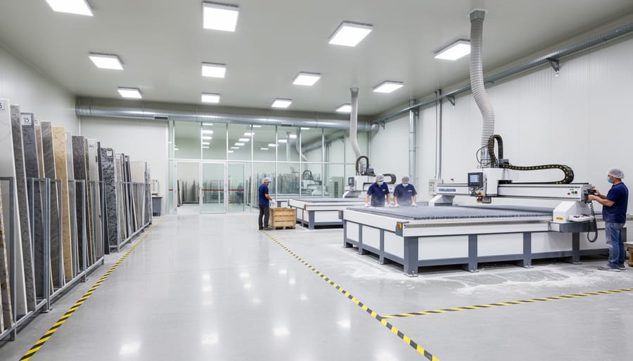
Premium natural stone fabrication facilities now recognize similar principles apply to their work, though at different scales. High-end countertop fabricators increasingly install climate-controlled shops where temperature swings won’t cause adhesives to cure unevenly or resins to develop inconsistent color matches. Dust extraction systems keep silica particles from settling on freshly polished surfaces where they would create scratches during handling.
The most advanced stone shops separate their fabrication zones by process. Cutting happens in isolated areas with dedicated ventilation. Polishing and finishing occur in cleaner spaces where airborne grit won’t contaminate the work. Assembly and quality inspection take place in controlled rooms approaching workshop-grade cleanroom standards.
Water quality matters too. Just as semiconductor fabs use deionized water to prevent mineral deposits during wafer cleaning, sophisticated stone fabricators filter their water supplies to avoid hard water staining on light-colored materials like white marble or quartzite. They’ve learned that controlling the environment means controlling the outcome, reducing rework and delivering more consistent quality to clients who expect perfection.
Surface Treatment and Finishing
In both semiconductor manufacturing and stone processing, surface treatment represents the final transformation that determines whether a product meets exacting specifications. Chemical mechanical planarization (CMP) in semiconductor fabs uses a precisely controlled combination of chemical slurries and mechanical polishing to achieve angstrom-level flatness across silicon wafers. This dual-action approach, chemical reaction softening the surface while mechanical abrasion removes material, mirrors the sophisticated finishing techniques employed in advanced natural stone fabrication methods.
Stone fabricators similarly combine chemical and mechanical approaches to achieve desired surface characteristics. Diamond abrasive polishing progressively refines the surface using finer grits, while chemical treatments like densifiers penetrate the stone matrix to increase hardness and reduce porosity. The parallel extends to quality metrics: semiconductor manufacturers measure surface roughness in nanometers, while premium stone fabricators increasingly use glossmeters to quantify polish levels rather than relying solely on visual assessment.
Both industries recognize that surface treatments serve dual purposes, functional performance and aesthetic appeal. Semiconductor CMP ensures proper electrical contact between circuit layers and creates the ultraflat surface required for subsequent photolithography steps. Stone finishes likewise balance practical needs (slip resistance, stain resistance, ease of maintenance) with visual impact. A honed marble floor offers better traction than polished but sacrifices some depth of color. A flamed granite exterior provides weather resistance through increased surface texture.
The semiconductor industry’s obsession with process repeatability offers a blueprint for stone fabricators aiming for consistency. CMP tools monitor pressure, slurry flow rate, pad conditioning, and processing time to deliver identical results across thousands of wafers. Stone professionals adopting similar process controls, documenting pad pressure, chemical dwell times, and number of passes per grit level, can achieve the consistency that distinguishes premium work from adequate results. The principle remains universal: surface quality cannot be inspected into a product; it must be built in through controlled, repeatable processes.
Lessons for Natural Stone Fabrication
The semiconductor industry’s commitment to methodical excellence offers stone fabricators concrete pathways to elevate their craft. While the materials and scale differ dramatically, the underlying principles of precision, consistency, and continuous improvement translate directly to natural stone processing.
Start with comprehensive process documentation. Semiconductor fabs maintain detailed records of every parameter for each production run, creating a traceable history that enables troubleshooting and refinement. Stone fabricators should document slab characteristics, cutting parameters, tooling choices, and finishing sequences for each project. This creates a knowledge base that transforms experienced fabricators’ intuition into repeatable procedures that newer team members can execute reliably. When a particular granite responds beautifully to specific polishing compounds and speeds, that information becomes institutional knowledge rather than disappearing when skilled workers retire.
Yield optimization represents another direct application. Semiconductor manufacturers track defect rates and material waste with obsessive precision, analyzing patterns to identify root causes. Stone shops can implement similar process optimization strategies by measuring remnant sizes, tracking which slab types produce the most usable pieces, and analyzing where in the workflow defects typically appear. A fabricator who discovers that 15% of their quartzite edge chips occur during a specific handling transition can redesign that step and immediately improve finished product rates.
Contamination prevention deserves heightened attention for high-end installations. While stone fabrication doesn’t require semiconductor-level cleanrooms, the principles apply. Designate separate areas for different operations. Keep cutting zones away from polishing stations. Establish protocols for tool cleaning between different stone types. Consider how residual oils from one stone might affect the finish of the next piece on your polishing line.
Automation opportunities exist even in custom fabrication environments. Repetitive tasks like edge profiling, sink cutouts, or standard measurements can be automated or semi-automated, freeing skilled craftspeople for work requiring judgment and experience. The semiconductor industry automated the routine to enable human expertise where it matters most.
Finally, adopt precision measurement as standard practice. Invest in digital measuring tools and establish tolerance specifications for different project types. Measure at critical control points rather than only at final inspection. This creates early warning systems that catch problems while they’re still correctable, the same philosophy that makes semiconductor manufacturing economically viable despite its complexity.
At first glance, fabricating semiconductor chips and processing natural stone appear worlds apart. Yet examining these manufacturing processes side by side reveals shared commitments to precision, methodical material transformation, and uncompromising quality standards. Both industries take raw materials with inherent variability and apply sophisticated techniques to create products that meet exacting specifications.
The semiconductor industry’s success stems from relentless process refinement, exhaustive documentation, and a culture where tolerances measured in nanometers matter as much as eliminating defects that human eyes cannot see. Stone fabricators working with granite countertops or marble installations operate at different scales, but the underlying philosophy remains identical: understanding your materials, controlling your environment, and maintaining consistency through documented procedures.
What sets exceptional stone professionals apart is their willingness to learn from industries that have perfected aspects of manufacturing they are still developing. Temperature and humidity control. Contamination prevention protocols. Statistical process control. Automated inspection systems. These semiconductor manufacturing principles translate directly into higher yields, fewer customer complaints, and more efficient operations in stone fabrication shops.
The most successful fabricators recognize that natural stone’s beauty and durability deserve processing methods as sophisticated as the material itself. Whether cutting silicon wafers or shaping quartzite slabs, manufacturers who embrace precision engineering, invest in proper equipment, and commit to continuous improvement consistently deliver superior results.
Cross-industry learning does not mean abandoning the craft traditions that define natural stone work. It means respecting those traditions enough to pair them with modern manufacturing excellence, creating products that honor both the material’s natural character and the customer’s expectations for flawless execution.